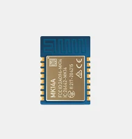
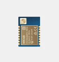
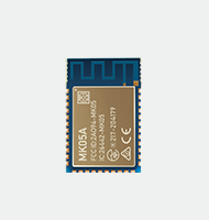
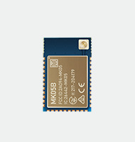
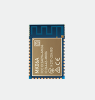
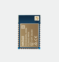
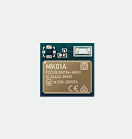
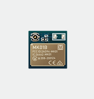

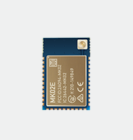
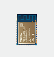
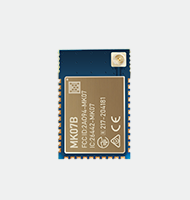
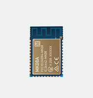
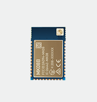
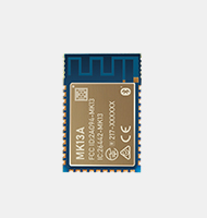
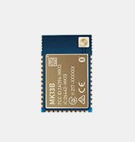
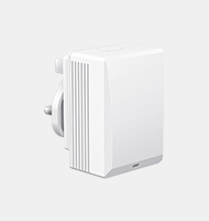
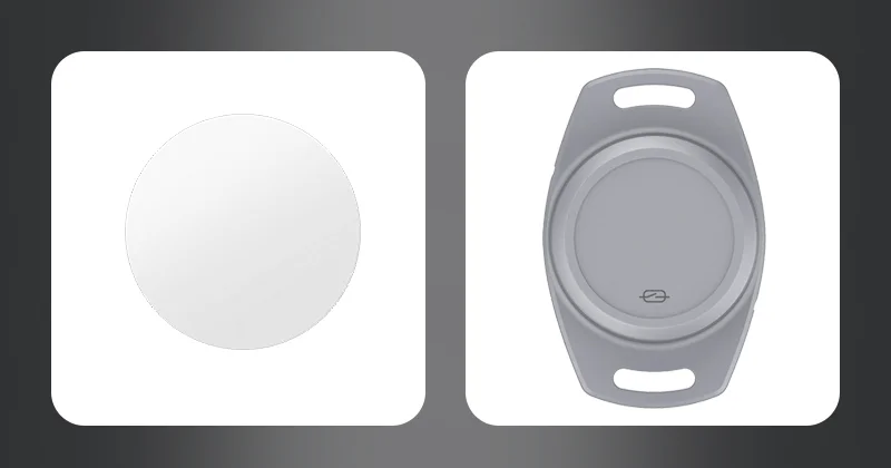
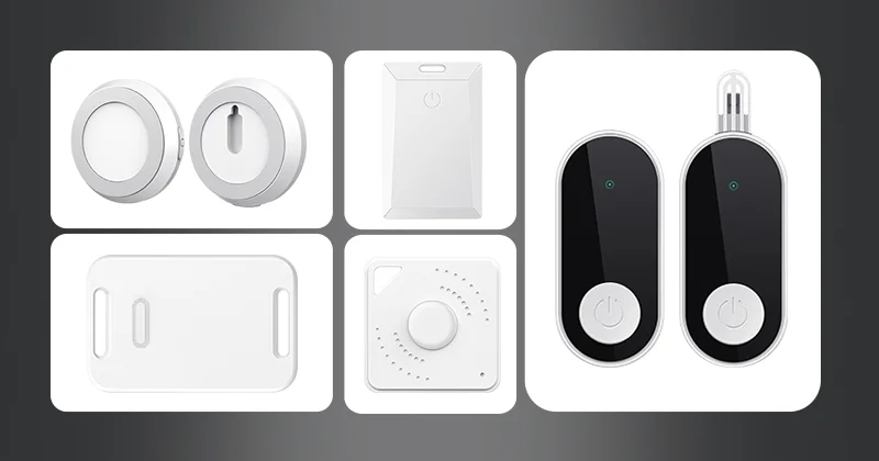
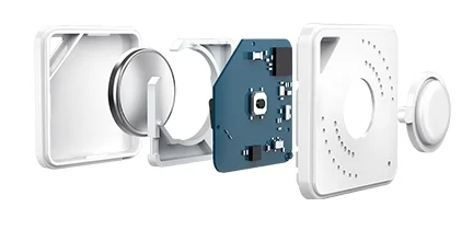
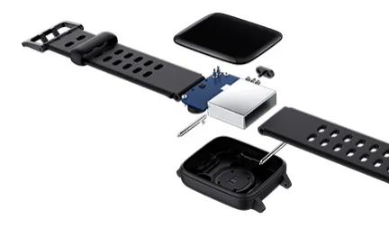
Our Beacon Devices
The MOKO beacon come in a variety of series which are divided into the H series, M series and the W series.
Some examples or Moko Beacon are listed below:
| M1 Coin Beacon | M2 Beacon |
| nRF52810 chip | Nordic nRF52811/nRF52810/nRF52832 |
| ABS + PC material | ABS+PC |
| Single Red LED | Single Red LED |
| Apple iBeacon | Apple iBeacon |
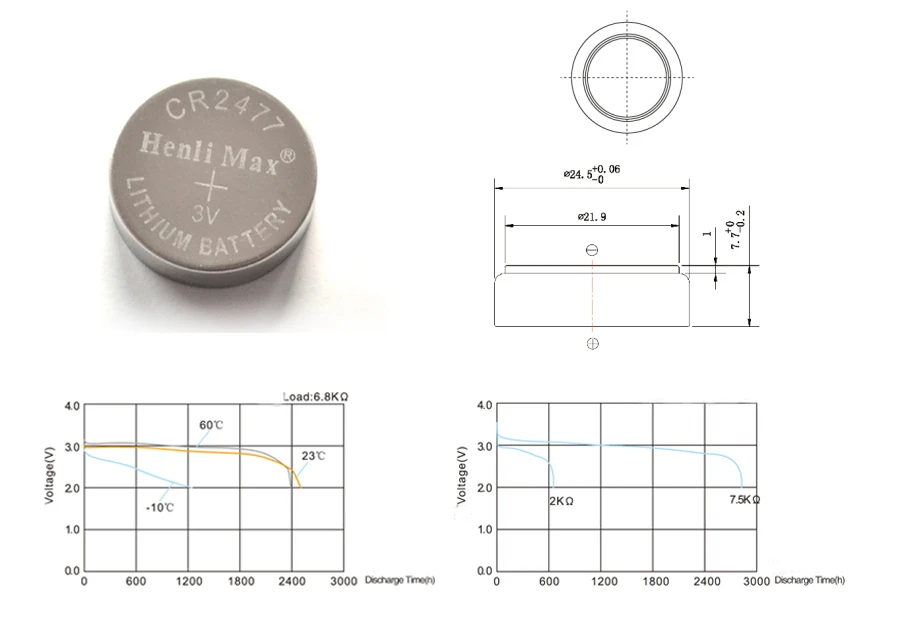
| Replaceable 220mAh CR203 battery | Replaceable 1000mAh CR2477 Battery |
| H1 Beacon | H2 Beacon | H2A Beacon |
| Main chips nRF52832 and nRF52810 | Main chips nRF52832 and nRF52810 | Main chip nRF52810 |
| Made of ABS +PC+TPU materials | Made of ABS +PC+TPU materials | Made of ABS +PC+TPU materials |
| Single Red LED | Single Red LED | Single Red LED |
| Apple iBeacon | Apple iBeacon | Apple iBeacon |
| Replaceable 220mAh Lithium coin CR2032 battery | Replaceable 1000mAh lithium coin CR2477 battery | Replaceable 1000mAh lithium coin CR2477 battery |
| H3 Beacon | H4/H4 Pro Sensor Beacon | H5 RFID Beacon |
| Main chips nRF52832 and nRF52810 | nRF52832 chip | nRF52810 chip |
| Made of ABS materials | ABS + PC and PMMA material | Made of ABS +PC+TPU materials |
| Single Red LED | 1 green and 1 Red LED | Single Red LED |
| Apple iBeacon | Apple iBeacon | Apple iBeacon |
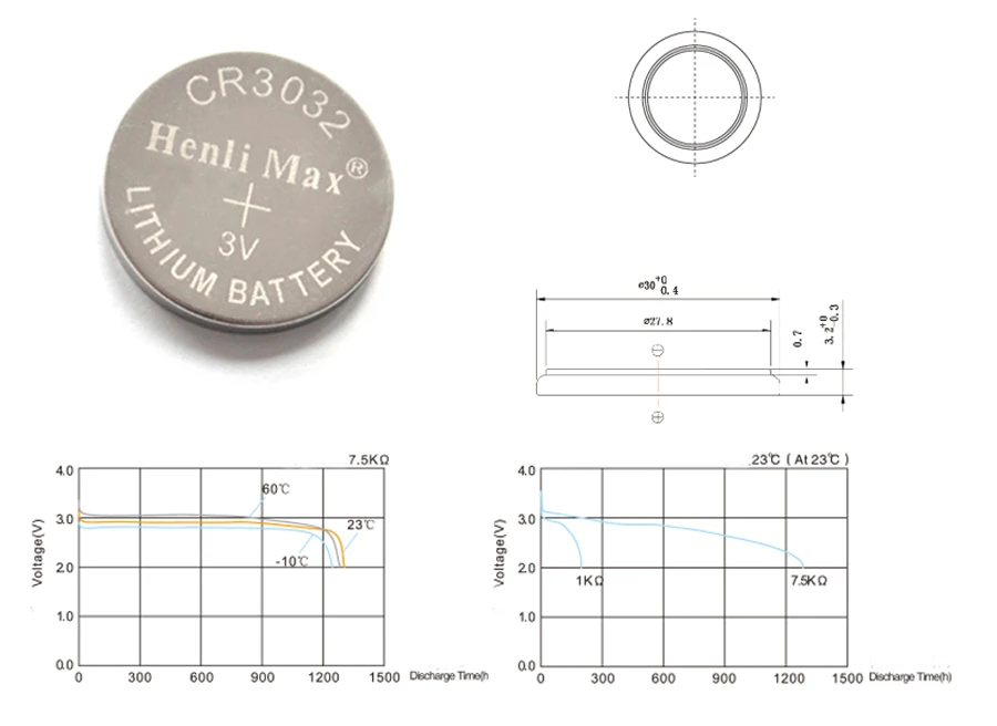
| Non-replaceable 800mAh Li-MnO2 battery | Replaceable 1200mAh AAA battery | Replaceable 550mAh CR3032 battery |

| W2 Beacon | W3/W3B Beacon | W3 Pro beacon | W5 Beacon | W6 Beacon |
| Nordic nRF52832 | Nordic nRF52810/ nRF52832 | Nordic nRF52810/ nRF52832 | Nordic nRF52832 | Nordic nRF52811/ nRF52810/ nRF52832 |
| PC+TPU | ABS+PC | ABS+PC TPE | PC+Cover glass ,TPU | ABS+PC |
| RGB LED | Single Red LED | Single Red LED | RGB LED | Single Red LED |
| Apple iBeacon | Apple iBeacon | Apple iBeacon | Apple iBeacon | Apple iBeacon |
| Rechargable 80mAh Lithium | Replacable 220mAh CR3032 battery | Non replacable 220mAh CR3032 | Rechargable 230mAh Lithium battery | Replacable 220mAh CR3032 |
Enclosure materials
As you can see from the above-listed Moko beacon series. MOKO beacon enclosure cases are made from one, or the combination of two or more of the under-listed enclosure materials:
- ABS (Acrylonitrile-butadiene-styrene)
- PC (Polycarbonate)
- PMMA (Acrylic)
- TPU (Thermoplastic polyurethane)
Why we choose them
ABS
- It can be pigmented easily (that is, it readily absorbs colors through the pigmentation process).
- It’s easily manipulated with machines and simple tools
- It is a great insulator
- Has lightweight and is impervious to most chemical spills
PC (Polycarbonate)
- It’s tough and can withstand considerable impacts without much damage
- Can operate optimally in a wide range of temperature
- Its processed form is very attractive
- It’s cost-effective for extreme-environment usage
PMMA (Acrylic or Plexiglas)
- It can be recycled and reused without degradation
- It is scratch-resistant
- It comes in different shades of beautiful colors
TPU
- It is highly flexible and durable
- It has a wide range of sizes and colors
- It exudes very minimal fumes during printing
In addition to these advantages, these materials have their specific cons. Therefore, we combine two or more of the materials in our beacons to complement their functions and also make up for their respective inefficiencies. This makes MoKo beacon products of the very best materials.
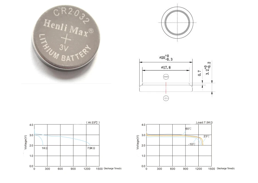
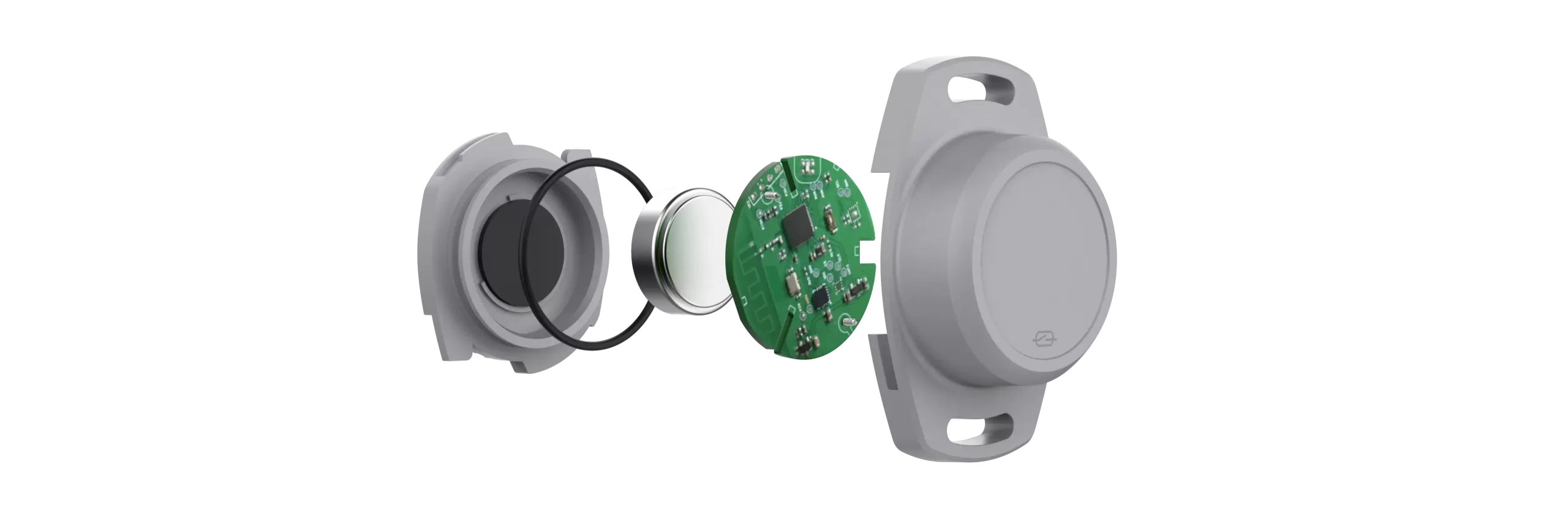
Batteries
Different types and kinds of batteries are used in these beacons, ranging from replaceable to non-replaceable batteries. Which could either be Coin cell (or button) batteries, AAA batteries are another MoKo battery type though, AA batteries are also used. And, how long each battery lasts depends on factors such as transmitting, advertising interval, and also beacon processor chip type, among others.
AA and AAA batteries are larger, bulkier, and are used on much larger beacons which provide higher power and also have higher power consumption. While coin cell or button batteries are much smaller, sleeker, and can fit into smaller beacons which have reduced power consumption. Coin cell batteries are lithium-ion cells and they can provide up to 1000mAh of power and are also much more reliable than the others.
Batteries could also be divided into single-use or rechargeable batteries. The single-use batteries have a particular charge and are used until it runs out of power and is then disposed of. The usual cheapness and low self-discharge rate are the two most pronounced advantages of single-use batteries, and they are also very widely available. A disadvantage however is that they cannot be re-used.
Rechargeable batteries are batteries that are made to be used and then, can be recharged over and over again, continuously. An advantage of this kind of battery is that they are very long-lasting and they also generate less waste than single-use batteries.
Here are some tips on choosing the right battery for your beacon:
- Check which battery the device uses and continue with that kind.
- Weigh the pro and cons of the various batteries and decide which is best for your device and suits your needs.
The main choice of the MOKO beacon is the Coin cell single-use batteries because they have a low power consumption and discharge and also have extended battery life when compared to others.
Antennas
An antenna is an important part of a beacon and the right antenna will significantly improve the performance of the device. The most common types of antennas are PCB (Printed Circuit Board) antenna, Ceramic antenna,Chip antenna, FPC antenna and the Whip antenna.
PCB Antenna
This antenna comprises a trace that is drawn on a Printed Circuit Board. The types of trace on the board might also vary depending on some factors which include the space required for it. The trace is placed on the board in order to facilitate wireless communication and can sometimes be time-consuming to produce.
Advantages of the PCB antenna include:
- The trace antenna is usually embedded during manufacturing.
- The antenna has a wide bandwidth
- It has a strong and reliable network
- Their two-dimensional structure helps limits their bulkiness
Disadvantages of the PCB antenna include:
- They take a long period and are challenging to design
- They require much more space than other antennas
- They can sometimes be easily interfered with by the environment or weather
- They are expensive to make
- No changes or modifications can be made to the antenna after manufacturing.
Chip antenna: this kind of antenna requires a small space to be implemented. They can also be integrated with the Printed Circuit Board to give out high-frequency electromagnetic waves, which have a limited range.
Advantages of the chip antenna include:
- It is cost-effective
- Their properties and function can be configured in many different ways
- They are small in size
- They are less prone to interference from the environment
- They are easy to configure, modify or replace.
Disadvantages of the chip antenna include:
- They have an increased initial cost
- When compared to a Printed Circuit Board trace antenna, it is a little behind in terms of performance.
Whip antenna: This antenna majorly consists of a thin rod or a flexible wire connected to a transmitter. These kinds of antennas are usually flexible so as not to easily break when disturbed or moved.
Advantages of the whip antenna include:
- They are usually small in size
- They have a large bandwidth
- They are very easy to build and configure
- They are very sensitive
- They are resistant to electrical noise.
Disadvantages include:
- For better sensitivity, the rod/wire has to be at an increased height.
- For better performance, the antenna has to be located on a good ground plane.
Ceramic antenna:Some beacon models (such as H1, H5, W2) use ceramic antenna, which has stable parameters, small size and does not need to spend a lot of design effort.
FPC antenna:There are also some models (such as W5) using FPC antenna,which is based on the antenna design manufacturers for targeted design, this kind of antenna applicability is narrow, each model should be designed separately.
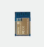
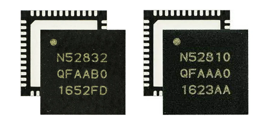
Chips used in beacons
The two major chips used in the MOKO beacon are the nRF52832 and nRF52810 chips.
The nRF52832 chip is a powerful multiprotocol chip that is used in a lot of Bluetooth and wireless devices because of its high-speed feature which supports a speed of up to 2mbps and also supports Bluetooth Low Energy (BLE) while offering a very good memory for both the Flash and the RAM. This chip is built around an Arm Cortex M4 CPU with a 64MHz floating-point unit. It also has an adaptive power management system which enables it to possess a very low energy consumption feature.
The nRF52810 chip is another member of the nRF52 and also features a CPU that uses ARM Cortex M4 and also uses the same architecture as others in its group, which supports easy migration and use from one chip to the other. It includes features like
- The 192kb flash with a 24kb memory
- a quadrature demodulator
- a programmable output power
- a high speed of SPI 8MHz
- an on-chip DC buck converter
- an easy DMA for connection with digital interfaces
- a Programmable Peripheral Interconnect
And has various applications and uses like in Medical and Fitness Sensors, toys, and also remote controls.
Waterproof Levels
The Ingress Protection ratings are used to measure the MoKo beacon waterproof levels. This kind of rating groups and rates the amount of protection against potentially damaging threats such as dust, accidental contact, and water. IP ratings come in a format such as ‘IP 65’, whereby the first number signifies its protection from dust and dirt, while the second number signifies its protection or resistance to water. The MOKO beacon has levels ranging from IP65, IP66, and IP67, which are defined as follows:
- IP65: This level signifies that the beacon is protected against water jets and water sprayed by a nozzle (6.3mm). The test period for this is 15 minutes; the water volume is 12.5 liters per minute, while the water pressure is 30kPa at a distance of 3m.
- IP66: This level signifies that the beacon is protected against powerful water jets and water sprayed by a nozzle (12.5mm). The test period for this is 3 minutes; the water volume is 100 liters per minute, while the water pressure is 100kPa at a distance of 3m.
- IP67: This level signifies that the beacon is protected against water immersion of up to 1m. The test period for this is 30 minutes;
PCB manufacturing techniques
The process of manufacturing a PCB is a complex one and it involves a lot of steps to be carried out accurately to arrive at the finished product. The PCB manufacturing process is as follows:
- The first step is the design process. This is where the designer or manufacturer lays down an outline for the PCB and also identifies its requirements. Design software can also be used and a commonly-used one is Extended Gerber. This software encodes all the useful information needed by the designer and it also goes over it numerous times to ensure that no errors are present.
- After the design has been made, it still needs to be checked numerous times to ensure that everything is in place and that there are no missing important components if it has been adequately checked and no mistake can be found, the design can then be advanced to the next stage.
- A printer known as the plotter printer is used to print out the design of the PCB. This printer makes a special film of the design and the layers of the board are represented in black and clear ink. The black ink represents the copper circuits while the clear ink represents the non-conductive areas of the board. After the printing, the films are arranged and holes are punched through them to align them.
- The manufacturer then prints the design onto a piece of laminate, while copper is added to it. Then the laminate is covered by a film that is photo-sensitive (known as the resist) and lined up accordingly, using the holes punched in for alignment. When they are conveniently lined up, an ultraviolet ray is passed through to harden the resist, and then the board is washed with an alkaline solution to wash away the remaining and unwanted photo-resist. It then goes through pressure washing and is then left to dry.
- After drying, the necessary copper on the board is covered, while exposing the rest to a chemical that removes unwanted copper from the board, and leaves only the required or wanted amount.
- After the adequate etching and removal of unwanted copper, the board is then cleaned and then aligned according to layer. The layers are placed on a machine that drives a pin through the holes in the various layers of the board.
- After the layer alignment, an automated optical inspection is carried out to ensure that no mistakes are present. This process is very important as this is the last stage in which you can make changes to the board before they are joined together permanently and no further changes or mistakes can be fixed. This inspection is carried out by a machine.
- After the layers have been checked and are found to be without defects or mistakes, the various layers are then ready to be fused. The layers are fused like a sandwich and are done on a special press table with the aid of metal clamps. A layer of pre-coated epoxy resin is placed first, followed by a layer of substrate, and then a copper foil layer which is also proceeded by more resin sheets and then finally covered with a piece of copper called a press plate. After these have been stacked on one another, it is then mechanically pressed and fixed properly. Then the stack is taken to a laminating press to apply heat and pressure to the various layers to keep them together.
- The stack is then passed through an x-ray machine which checks and locates drill spots and is then drilled, removing excess leftover copper.
- Then the next step is the plating, whereby the board is cleaned and then a chemical is used to fuse the different PCB layers and it is then bathed in other chemicals, one of which includes copper.
- Another layer of photo-resist is then applied, in addition to the one applied earlier. However, this photo-resist is only applied to the outer layer before it is then imaged again by a machine.
- An outer layer etching is then undergone, and in this process, additional excess unwanted copper is removed with a solvent. This then prepares it for another automated Optical inspection with a machine.
- The outer layer then undergoes another round of automated optical inspection to ensure that the design matches up to what was produced and that all excess copper is removed to prevent improper electrical connections.
- The panels are then thoroughly cleaned before a solder mask is applied. Each panel is covered by an ink epoxy and solder mask film and then it is put in an oven for curing.
- After this, relevant important information is then written and printed on the board. Information like company ID numbers, warning labels ad manufacturers logos is included.
- Then it is plated with conductive materials, as well as being tested to ensure that it performs its functions adequately, and after checks, is then packaged and sent off for sale and delivery.
Test Process of MOKO beacon
Testing is an important aspect because it verifies if the device is working properly as it should be. All Beacons and beacon types can be tested at any time; this testing can be done using the self-test function. Operational testing, however, sometimes require permission and approval, and the following requirements have to be met before approval is given:
- The beacon is to be coded with the TEST protocol.
- The 121.5/243 MHZ signal should be disabled.
- Prior notice should be given.
In the case of manufacturers testing MOKO beacon, some of these requirements also have to be met:
- The test should not be for more than a period of 15 minutes.
- The location of the test should be adequately provided.
- Prior notice of at least two days should be given.
- Beacon bursts should be limited.
- The test objective of the intended test should be stated
- The test description should be stated.
- The Beacon ID should be provided.
Testing processes of MOKO beacon are as follows:
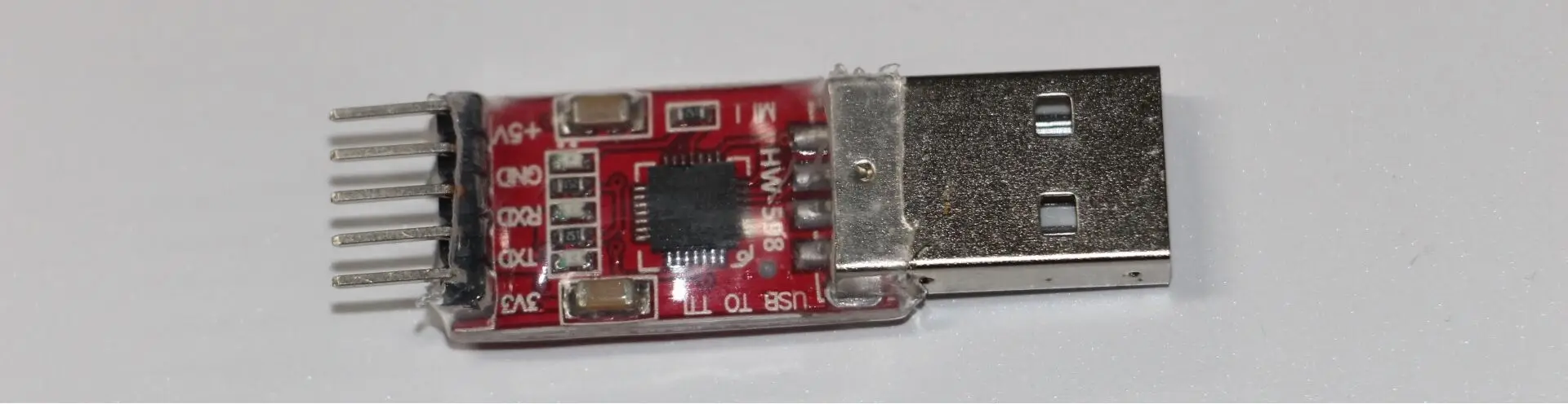
Prepare wiring and gauge
- Take a single PCBA with burned firmware and put it into the test rack. The test rack can be powered by an adjustable 3.0V-3.3V power supply. The red terminal on the back of the test rack is the positive terminal while the test rack’s negative terminal is represented by the black terminal.
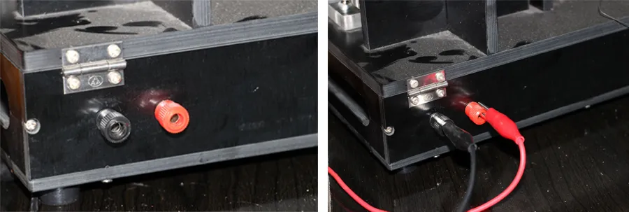
- Turn on the power switch of the fixture, and the pointer voltmeter indicates the power supply voltage of 3.0-3.3V (Note: the USB interface of the digital display ammeter needs to be inserted into the computer’s USB hole for power supply)
- Connect one end of the red USB to the serial port tool that has been connected with the wire to the USB end of the computer, and connect the other end to the test rack.
Operation steps
- Open Beacon serial port printing upper computer software
- Select the serial port number of the corresponding module, and click “Open serial port”.
- Place the single board PCB in the test rack, energize the PCB, and the PCB lamp flashes. After the lamp is off, the digital display ammeter will display a value of about 1mA.
- Click “Disconnect” and observe the digital display ammeter. It shows that the value below 100uA is in a state of jump, and it jumps repeatedly within the range of dozens of uA. The minimum jump below 20uA is required to be normal.
- If the digital display ammeter does not meet the above requirements, the PCB will be taken out for defective product treatment (generally caused by false welding caused by patch or material damage).
Printer installation wiring instructions
- Install the USB to the serial port tool and printer driver. USB to serial port tools and printer drivers have been stored in the driver folder; Use the printer power access, USB turn nine serial port connect the printer and computer. The blue light on the printer is always on after power on and the connection is successful.

The operation of the upper computer
- Open the “MOKO Beacon serial port to print upper computer software”.
- Select the production interface and fill in the batch order number.
- Select the serial port number of the corresponding module, and click “Open serial port”.
- Click “Import Configuration” and select the the.ini file in the folder.
Label printing operation
- The following operations shall be completed within 30 seconds after the push rod of the test stand is pushed down. If the operation is interrupted midway, please push the pushrod up and push the module down again.
- Place the single board PCB in the test rack, energize the PCB, and the PCB lamp flashes. After the lamp is off, the digital display ammeter will display a value of about 1mA;
- Click “Run” on the lower right side.
- The green character “success” appears in the window of the comparison result, and the sensor status is “OK”. If success occurs, the printer will print out the label. Check that the words on the printed sticker are centered above and below.
- When the display is successful, click “Disconnect” and click “Save”. Please note that each operation can only be clicked once to save, do not click twice!
Input device test
Long press the button on the fixture for 3S to shut down the device, and the LED will be on for about 2 seconds. The button is required to feel crisp without hysteresis, indicating that the button functions normally.
Send mail
- At the end of each test day, send the file “mysqliteDatabase” to the designated QA audit email address.
- The test supervisor will upload the reviewed order test data into a compressed file to the FTP server, and the file path is production data /1. Factory feedback data /1. Bluetooth MOKO Beacon
- QA will send the confirmed data to the business email.
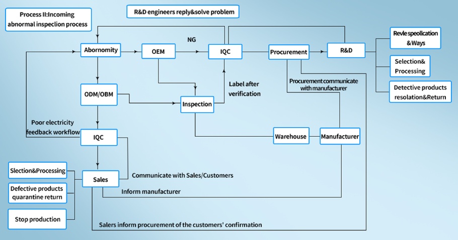
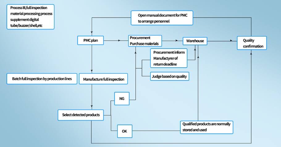
The Inspection process for MOKO beacon
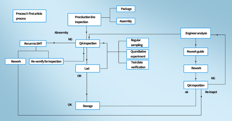
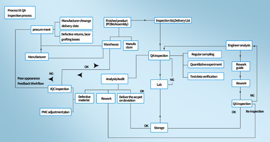
The inspection process for MOKO beacon is known as the First Article Inspection (FAI) and this is done when a person, who is usually authorized to do so, uses measuring equipment to measure and test one or more parts of the device to ensure that they are all working properly. They are then compared to the specifications and functionality listed by the client to see if they match up. The components selected for testing are usually selected from the first batch of products manufactured. Inspection is done for several reasons, some of which include:
- To verify and check the accuracy of the drawings with the final product manufactured
- To verify that the correct procedures for production were adhered to in the manufacturing of that product.
- To ascertain and make sure that the manufacturer meets the needs of production.
- To determine any minute or large shift in the location of the PCB.
- To identify if there are any possible changes or obstructions during the process of production.
The under-listed process involves:
- The first stage is to define the needs and requirements of the inspection. Why are you inspecting? What are you inspecting for? And also the requirements that have to be met by the products during the inspection have to be defined.
- The next step is the inspection plan where the inspector draws up a plan of the process through which the inspector intends to check the products.
- After the inspector has a plan, the inspector then proceeds to inspect the products.
- The products are judged based on their requirements, functionality, and quality, and if there are any defects within them. If a defect or error is found, it is then recalled and either sent back for modification and repair or it is destroyed.
- If the products pass the test without any hitches or complaints, the products are then approved to be sent for storage, delivery, or sale as the case may be.
- While testing the materials, the inspector prepares a detailed report of the whole process and operation, along with any potential mistakes or any defects spotted. The final compilation report is then sent to the manufacturer or whoever the inspector reports to. And, actions are taken from there, whether to proceed or to make some crucial changes.
What the Inspector checks
Some of a number of things which the inspector checks are:
- The quality of the products
- The quantity of the products produced
- The packaging of the product
- The connections, especially the electrical ones within the products
- The manufacturing procedure and processes.
- The hardware of the materials under review
When is an Inspection carried out?
An inspection is usually carried out during the first production run, or when the design of a product changes, to ensure that it still retains its functionality regardless of the change. Also if some factors of production should change, for example, the source of the raw materials, an inspection is required to ensure that it regains its quality.
An inspection is important and necessary because it helps retain the quality of the product, while also reducing waste as a result of production defects and also saves time by catching potential problems sooner.
Also, with the emergence of technology, computers are now being used to record and store crucial information digitally without having to record everything on paper, and also helps to generate instant reports immediately after the process of First Article Inspection.
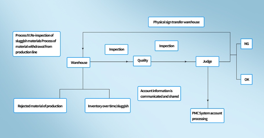
Production inspections are of two types
In due course of production: In this stage, the products are tested and inspected midway through the production process to identify errors early and prevented waste. This type is usually done and is ideal for large-scale product manufacture, and for products that have a high risk of defects.
The last stage Inspection: This type of inspection is usually carried out after the entire production and manufacturing process. What is now being inspected is the finished product to verify the safety and standards of the product.
Although the quality control and inspection process are very important in manufacturing, some companies might not be comfortable with that and often employ some tactics to avoid or reduce quality control interference.
Though we do not bunk inspection in any way, some companies do that. You need to avoid purchasing from any company that practices any of the under-listed shady tactics for them to avoid quality control.
Some Company might avoid inspection through some tactics
- Providing wrong factory address:
Some companies, in a bid to hide or mask the actual process or conditions of the production process, might give out a false address for the inspection to take place. They might stage a different location for the inspection which is quite different from the location the actual production takes place in.
- Limiting access to parts of the building
Even if the correct address for the production location is given, some companies might still want to limit the access of the auditor and prevent him/her from entering certain areas. The areas allowed might just often be the storage area or warehouse where the finished products are stored and another area allocated for inspection, which is different from the production area and they might usually be accompanied by factory workers or staff to prevent them from straying.
Not confirming a set date for inspection:
Another way some might try to avoid this is the instance where there is no set and confirmed date for the quality control and audition. The company usually reschedules several times over or might bring up a reason to avoid scheduling for a particular date.
Not providing the right equipment:
Although some auditors possess some testing and quality control equipment, a large chunk would have to be provided by the company for accurate reading of results and some might try to circumvent this by providing the inspectors with faulty or tampered equipment to give false readings or results favorable to the company. Other times, they might bring up an excuse of the equipment being unavailable at that particular time for one reason or the other.
Refusing some on-site testing:
Some companies might choose to not allow some specific testing to be done on-site as a result of one or two reasons.